Defect formation in two-dimensional MoS2 in very low voltage TEM likely caused by electronic excitations
March 20, 2020 - The role of electronic excitations for defect production at electron energies below the knock-on threshold is a long-standing question. Using a combination of atomically resolved data from the SALVE TEM and theoretical calculation researchers from the Helmholtz-Zentrum Dresden-Rossendorf and Ulm University revealed a new mechanism of defect formation below the knock-on threshold.
For a long time, scientists work to unravel mechanisms of electron beam damage in periodic solids due to inelastic effects. A combination of model calculation and experimental data now showed that excitations in the electronic system can create vacancies by ballistic energy transfer with electron energies that are much smaller than the knock-on threshold of the initial state. The new study indicates that an additional channel for the creation of defects for individual MoS2 layers in the range of 20–80 kV exists, which is relevant also for other semiconducting materials.
Evaluating defect production
Scientists have considered 3 mechanisms which can contribute to defect production: [1,2] (i) knock-on damage due to elastic electron scattering and direct impulse transfer from the electron to a target atom,[3] (ii) inelastic damage due to electron scattering and energy transfer to the electronic system (radiolysis )[4] and (iii) beam-induced chemical etching.[5] The first channel predominates at high electron energies and cannot occur below a certain threshold energy. Below the so-called knock-on threshold, the electron cannot transfer sufficient kinetic energy to displace the recoil atom. Therefore, the goal was to reduce the accelerating voltage in the TEM,[6] which was successfully achieved by maintaining atomic resolution after the development of aberration correctors.[7,8]
Recently, the discovery of two-dimensional (2D) materials[9] enabled more detailed studies of radiation damage. The new materials proved to be radiation-sensitive[10] and the ability to identify individual atoms in the TEM made it possible to quantify the damage by counting missing atoms[5,11] with high precision. However, the possibilities for investigation remained limited to a narrow window of accelerating voltages, usually between 60 and 80 kV, since no atomic resolution could be achieved for low voltages and the damage occurred too quickly for higher voltages.[12] It was therefore still challenging to distinguish and investigate the damage mechanisms (2) and as a result, no quantitative microscopic theory that describes the relationship between the electronic stimulus and the damage generation in periodic solids is available today. For instance, the generation of defects in inorganic 2D materials at voltages (e.g. 60 kV)[12] well below Uth ≤ 80 kV[13] has not yet been explained.[3] The new research did now combine for MoS2 the first principles simulations for the generation of defects with accurate measurements of the damage rate in the energy range below the knock on threshold of MoS2.
“Many research groups have already published papers analyzing possible mechanisms for the defect production below the knock-on threshold,” says Prof. Ute Kaiser, who led the TEM studies at Ulm University. “As atomic resolution is recently become available in the SALVE TEM at very low electron energies, we could for the first time provide an accurate measurement of defect production rates down to 20 kV and compare with model results.”
Electronic excitations: Insights from model calculations
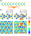
The model calculations showed that the lifespan of a core hole in for a fully symmetric 2D MoS2.is of the order of a few fs. The excitation was found to be only initially localized, but after a few fs it was found distributed over the entire system (Figure 1). The localization occurred on a lifetime, which is much shorter than the time of ~ 100 fs required to break a bond.
In their paper, the authors now proposed a new mechanism that can cause defect production below the knock-on threshold. Their model results showed that the behavior of the system looks completely different if the translation symmetry is interrupted, for example, by a defect that occurs. Physically, this is the situation in which an electron ballistically transfers some energy to the recoil atom and at the same time causes electronic excitation, or the excitation was previously generated in the system, as shown schematically in Figure 2.
While the energy to displace an atom in the ground state was found to be 7.1 eV, in agreement with previous calculations,[3] a clear drop in the threshold energy to 4.8 eV was found when an electron was in the excited state. For the double excitation, decreased further to 3.5 eV.
Radiation damage: Hard to quantify
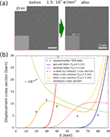
The model results can well explain the number defects that were created by the electron beam. The defects were counted by atomically resolved HRTEM of MoS2 at 20, 30, 40, 60 and 80 kV accelerating voltage before and after exposure to a known total dose. From these images, the displacement cross section σ could be determined for quantitative evaluation (Figure 3).
As a remarkable feature, it was first found that the experimental values of σ (Figure 3b) is smaller than at 30 kV, indicating a threshold voltage for defect formation. Neither the excitations alone nor the chemical etching (mainly associated with the generation of reactive species by removing H atoms from water molecules) can be responsible for this damage production, since the cross section of both processes decreases monotonically with voltage.
As a next step, the scientists calculated the total cross section σtot (E) as a sum of the knock-on damage processes of the ground states and the excited states. The lifetime of an excitation in a MoS2 sheet is approximately 1 ps.[14] For high current densities of 105–106 A/cm2, a two electron process is possible, where two electrons strike the same area with dimensions of approximately 10 × 10 nm2 during the lifetime of the excitation. It can displace the recoil atom from its position in the lattice, thereby lowering the binding energy and thus the displacement threshold. This indicated that the defect production rate (per number of impinging electrons) should be higher at high beam currents, which was also experimentally found in experiments on inorganic materials.
„Many aspects of electron beam-sample interactions remain to be explained, and new microscopes and models are currently pushing the boundaries of our understanding,“ Kaiser says „The newly discovered mechanism is relevant for a variety of semiconducting materials.”
Ressource: Kretschmer, S., Lehnert, T., Kaiser, U., & Krasheninnikov, A. V. (2020). Formation of defects in two-dimensional MoS2 in the transmission electron microscope at electron energies below the knock-on threshold: the role of electronic excitations. Nano letters, 20(4), 2865-2870, https://doi.org/10.1021/acs.nanolett.0c00670.
-
Susi, T.; Meyer, J. C.; Kotakoski, J. Quantifying transmission electron microscopy irradiation effects using two-dimensional materials. Nat. Rev. Phys. 2019, 1, 397– 405, DOI: 10.1038/s42254-019-0058-y
-
Egerton, R. F. Control of radiation damage in the TEM. Ultramicroscopy 2013, 127, 100– 108, DOI: 10.1016/j.ultramic.2012.07.006
-
Komsa, H.-P.; Kotakoski, J.; Kurasch, S.; Lehtinen, O.; Kaiser, U.; Krasheninnikov, A. V. Two-Dimensional Transition Metal Dichalcogenides under Electron Irradiation: Defect Production and Doping. Phys. Rev. Lett. 2012, 109, 35503, DOI: 10.1103/PhysRevLett.109.035503
-
Wei, X.; Tang, D.-M.; Chen, Q.; Bando, Y.; Golberg, D. Local Coulomb Explosion of Boron Nitride Nanotubes under Electron Beam Irradiation. ACS Nano 2013, 7, 3491– 3497, DOI: 10.1021/nn400423y
-
Meyer, J. C.; Eder, F.; Kurasch, S.; Skakalova, V.; Kotakoski, J.; Park, H. J.; Roth, S.; Chuvilin, A.; Eyhusen, S.; Benner, G.Accurate measurement of electron beam induced displacement cross sections for single-layer graphene. Phys. Rev. Lett. 2012, 108, 196102, DOI: 10.1103/PhysRevLett.108.196102
-
Linck, M.; Hartel, P.; Uhlemann, S.; Kahl, F.; Müller, H.; Zach, J.; Haider, M.; Niestadt, M.; Bischoff, M.; Biskupek, J.Chromatic Aberration Correction for Atomic Resolution TEM Imaging from 20 to 80 kV. Phys. Rev. Lett. 2016, 117, 076101, DOI: 10.1103/PhysRevLett.117.076101
-
Haider, M.; Uhlemann, S.; Schwan, E.; Rose, H.; Kabius, B.; Urban, K. Electron microscopy image enhanced. Nature 1998, 392, 768– 769, DOI: 10.1038/33823
-
Krivanek, O. L.; Dellby, N.; Lupini, A. R. Towards sub-Å electron beams. Ultramicroscopy 1999, 78, 1– 11, DOI: 10.1016/S0304-3991(99)00013-3
-
Novoselov, K. S.; Jiang, D.; Schedin, F.; Booth, T. J.; Khotkevich, V. V.; Morozov, S. V.; Geim, A. K. Two-dimensional atomic crystals. Proc. Natl. Acad. Sci. U. S. A. 2005, 102, 10451– 3, DOI: 10.1073/pnas.0502848102
-
Zhao, X.; Kotakoski, J.; Meyer, J. C.; Sutter, E.; Sutter, P.; Krasheninnikov, A. V.; Kaiser, U.; Zhou, W. Engineering and modifying two-dimensional materials by electron beams. MRS Bull. 2017, 42, 667– 676, DOI: 10.1557/mrs.2017.184
-
Lehnert, T.; Lehtinen, O.; Algara-Siller, G.; Kaiser, U. Electron radiation damage mechanisms in 2D MoSe2. Appl. Phys. Lett. 2017, 110, 033106, DOI: 10.1063/1.4973809
-
Lin, Y. C.; Björkman, T.; Komsa, H. P.; Teng, P. Y.; Yeh, C. H.; Huang, F. S.; Lin, K. H.; Jadczak, J.; Huang, Y. S.; Chiu, P. W.Three-fold rotational defects in two-dimensional transition metal dichalcogenides. Nat. Commun. 2015, 6, 6736, DOI: 10.1038/ncomms7736
-
Yoshimura, A.; Lamparski, M.; Kharche, N.; Meunier, V. First-principles simulation of local response in transition metal dichalcogenides under electron irradiation. Nanoscale 2018, 10, 2388– 2397, DOI: 10.1039/C7NR07024A
-
Docherty, C. J.; Parkinson, P.; Joyce, H. J.; Chiu, M. H.; Chen, C. H.; Lee, M. Y.; Li, L. J.; Herz, L. M.; Johnston, M. B. Ultrafast transient terahertz conductivity of monolayer MoS2and WSe2 grown by chemical vapor deposition. ACS Nano 2014, 8, 11147– 11153, DOI: 10.1021/nn5034746


