SALVE Cs/Cc-correction realized
August 09, 2016 - By pushing the usable aperture to the highest value ever reached in phase-contrast TEM imaging, the SALVE project completes the list of atomic-resolution TEMs. The SALVE III TEM operates in the range between 20 to 80 kV obtaining a resolution limit as small as 15 wavelenghts which is more than six times smaller than that of uncorrected TEMs.
Since the beginning of aberration-corrector technology, transmission electron microscopy (TEM) provides sub-Angstrom instrumental resolution provided that the specimen is not damaged by the electon beam [1, 2]. In order to avoid atom displacement by knock-on processes, the energy of the electron most stay below a characteristic threshold energy which is proportional to the mass of the atom [3]. Specimens consisting of light elements such as biological objects, polymers, and ceramics are in addition damaged by ionization processes even if the TEM operates at energies below the knock-on threshold [4 - 6].
In order to avoid knock-on damage at atomic resolution an aberration-corrected electron microscope is required which must operate at acceleration voltages as low as 80kV for many materials. Such a TEM was first completed in 2005 [7]. As a result, the exposure time could be increased significantly enabling atomic resolution for a variety of objects.
However, experiments have shown that this voltage must be reduced even further for resolving the atomic structure of interfaces and defects in materials composed of light elements. In order to reach atomic resolution for these materials, the SALVE project [8] was launched in 2009. The SALVE microscope operates at low voltages in the range between 20 and 80 kV below the knock-on threshold of the object. Unfortunately, for achieving atomic resolution at these voltages, the chromatic (Cc) aberration must be eliminated in addition to the spherical (Cs) aberration (see blue boxes at the end of the news article for an explanation). Without Cc correction, the minimum achievable resolution limit is about 0.2nm at these low voltages [9].
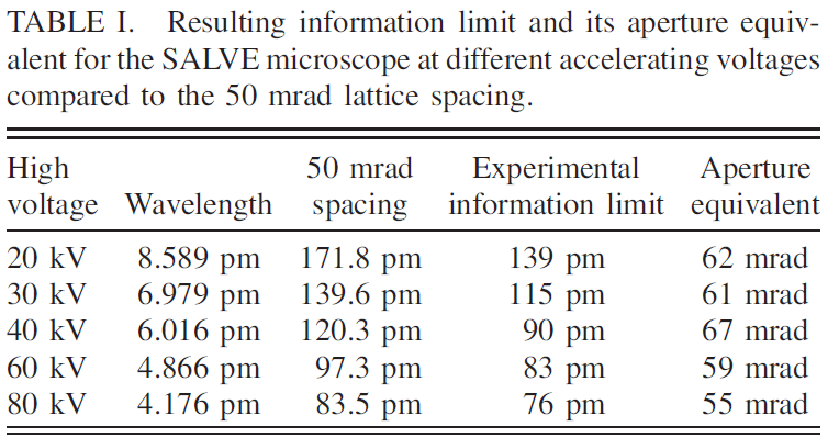
In the journal Physical Review Letters, the scientists of the SALVE project now report the successful implementation of the novel aberration corrector which provides an instrumental resolution limt of 0.76 Å - 1.40 Å in the range 80 – 20 kV (Table 1) [†].
"We were able to achieve the new resolution record due to our latest understanding of resolution-limiting factors in electron microscopy and by applying the improved understanding for the optimization of the corrector", said Prof. Max Haider, director of CEOS GmbH which is the world leader in corrector-development. The SALVE corrector is based on an early design of Prof. Harald Rose and his student Mathias Kuhn in 1992 [10]. Prof. Rose, who has a consultative role in the SALVE project, had initially suggested this corrector for realizing an electron optical aplanat which is free of primary chromatic, spherical, and off-axial aberrations, as required by the SALVE microscope. During the evaluation phase of the SALVE project (SALVE I, 2009 - 2011), the researchers concluded that this design is optimal for the SALVE corrector, because it provided by far the best performance of all investigated corrector designs. "I had completely forgotten this design over the years because the simultaneous correction of these aberrations was not necessary at the standard voltages above 80 kV used in TEMs so far" said Prof. Harald Rose. In the following phase "SALVE II" from 2011 - 2014, the corrector was developed, and in Phase III from 2015 - 2016 it was optimized and integrated into the microscope. "That the third phase could be so successfully completed is also due to the enormous commitment of SALVE III partner FEI Company which supplied and developed the microscope column", said Professor Ute Kaiser, principal investigator of the SALVE project.
Improved understanding of resolution limits in the TEM
Important progress has been made in the understanding of resolution limiting processes and parameters in the TEM in the last years, primarily by the members of the company CEOS. In the new publication the scientists explain in detail the most important parameters which affect the information limit. They are the spatial coherence of the illumination system, focus spread in the imaging optics caused by instabilities of the electromagnetic fields, and image spread resulting from Johnson noise [11]:
- The information-dampening effect due to partial spatial coherence is eliminated by the correction of the spherical aberration. It has first been experimentally demonstrated in 1998 [1] that Cs-correction improves the resolution of an electron microscope.
- The chromatic aberration transforms the energy spread of the electron source and the instabilities of the accelerating voltage and the lens fields into a focus spread. This focus spread is the main limitation for low-voltage TEM imaging regardless if the spherical aberration is corrected or not [12]. Apart from the primary chromatic aberration, the secondary chromatic aberration must also be sufficiently reduced at low voltages, as has been demonstrated in 2010 [13].
- After Cc correction, an additional focus spread—caused by instabilities of the focusing elements due to noise from the electronics’ supplies—remains, which must be reduced by using ultra-high quality electronic voltage and current sources [14] and ultra-low environmental noise, which must provide by a mechanically and electromagnetically shielded room.
- Stochastic beam deflections that are generated by every conductor (both magnetic and nonmagnetic, "Johnson noise" [11]) result in a resolution-limiting image spread.

Improved resolution due to improved understanding of resolution limits
To avoid the deleterious effects resulting from the instabilities of the electromagnetic fields, all currents and voltages must be kept extremely stable. To reduce the Johnson noise, the electrons’ ray path and the shape of the metal parts close to the beam are optimized [11]. A trade-off between the bore of the multipole elements, the lens gaps, and the liner tube diameter has been made, that enables the required correction strength and focusing power and, at the same time, prevents the electron beam from suffering too much image spread. These measures are at the edge of technological feasibility in that, for example, the magnetic materials in the multipols were excited close to saturation. Fig. 1 shows a photograph of the corrector and the schematic path of the paraxial rays. Details about the corrector and the microscope are available at the end of this news article.

Achievements
The SALVE corrector has been designed in such a way that the round aberrations, i.e., defocus C1 and spherical aberrations of third-order C3 and fifth-order C5 are tuned to specific values to establish a uniform phase contrast transfer function (PCTF). Moreover, all non-circular aberrations are reduced to such an extent that they do not prevent a sufficiently uniform phase surface [15]. The measured 20 kV phase plate in Fig. 2(f) indicates that this challenging task has been accomplished with the SALVE corrector. Moreover, off-axial aberrations including off-axial coma are tuned sufficiently small to provide a large field of view such that each object point is imaged in the same way regardless of its position in the object plane.
Measures to quantify the resolution are the Young’s fringe resolution test (Fig. 2) or the paraboloid method [16 – 19]. Both tests match and demonstrate that the SALVE goal of a usable aperture of 50 mrad has been reached and even exceeded for the whole voltage range (Table 1). The results will also be beneficial for the improvement of CC-correctors developed at a time before the resolution-limiting effect of Johnson noise was discovered.

A big step foreward for all sciences that use sensitive materials
With the new corrector, the resolution for graphene and MoS2 at 30 kV is comparable to the current state of the art at 80 kV. This is due to the large effective aperture of the instrument as well as due to increased scattering of the electrons at lower energies. The SALVE III microscope delivers for the first time images of an edge configuration in graphene because it remains fixed when imaged at 30 kV, whereas it is unstable under an 80 kV electron beam [20, 21].
Furthermore, images of free-standing monolayers of graphene and MoS2 at an accelerating voltage of 30 kV show, in good agreement with simulations, a strongly improved single-atom contrast (Figure 3). In the raw experimental images (1 s exposure time, 2048 × 2048 pixels frame size) the accumulated electron doses are 2.5 * 106 e−/nm2 and 3 * 105 e−/nm2 for graphene and MoS2, respectively. The diffractogram of graphene, which is a measure for the resolution, reveals reflections up to third order, corresponding to 107 pm. For MoS2, even the fourth-order reflections, i.e., 102 pm, can be detected in the diffractogram. It is possible to identify the single carbon atoms in the hexagonal lattice even under those dose-limited conditions. Moreover, molybdenum can clearly be distinguished from the two sulfur atoms, which are located underneath each other in this crystal projection, thus low voltages of 30 kV will not only allow for detecting single atoms and point-defect structures but also to determine their chemical nature.
The scientists from CEOS GmbH, FEI Company, and Ulm University successfully demonstrated the functionality of a TEM corrector for geometric and chromatic aberration correction for voltages from 20 to 80 kV. The achieved resolution at 40 kV corresponds to only 15 times the electron wavelength. This is a new record in phase-contrast TEM imaging. Furthermore, the correction of chromatic aberration opens up new opportunities for analytic imaging because large energy windows are almost equally well focused at the image plane. The demonstrated information limit of 90 pm at 40 kV corresponds to a maximum aperture angle of 67 mrad. Between 40 and 80 kV, sub angstrom resolution has been obtained. At 30 kV, the stability and resolution of the complete system (microscope and corrector) is more than sufficient to resolve single atoms in raw TEM images. At the current lowest-possible voltage of 20 kV, a resolution better than 0.14 nm can be achieved allowing even for atomic or near-atomic imaging. This is a huge step forward towards materials analysis on delicate, beam-sensitive objects; the SALVE microscope now combines both the desired resolution and the beam energy below knock-on threshold at the same time.
Another object of the SALVE project is to determine the optimum voltage for different materials and scientific objectives. With decreasing voltage ionization damage - known as radiolysis - increases. Therefore, another aim of the SALVE project concerns the reduction of ionization by improved sample preparation [22, 23]. The best choice of the electron energy depends on each individual sample’s compromise between ionization and knock-on damage [24]. "With the new SALVE III microscope scientists can now examine for the first time the sample with atomic resolution at electron energies in the range between 20 and 80 keV. This possibility is a great step for electron microscopists and all sciences which are using electron microscopy," says Prof. Ute Kaiser.
More details about Rose's contributions to hardware aberration correction including other pioneers works can be found here.
Highlighted Topics
Why do low voltages need CC correction?

Details about the corrector and the microscope
Resource: Linck, M., Hartel, P., Uhlemann, S., Kahl, F., Müller, H., Zach, J., Haider, M., Niestadt, M., Bischoff, M., Biskupek, J., Lee, Z., Lehnert, T., Börrnert, F., Rose, H. H. & Kaiser, U. A. (2016). Chromatic Aberration Correction for Atomic Resolution TEM Imaging from 20 to 80 kV. Physical Review Letters, 117: 076101, doi: 10.1103/PhysRevLett.117.076101, [PDF], see also the supporting information.
Haider, M., Uhlemann, S., Schwan, E., Rose, H., Kabius, B., & Urban, K. (1998). Electron microscopy image enhanced. Nature, 392: 768-769, doi: 10.1038/33823
Kisielowski, C., Freitag, B., Bischoff, M., Van Lin, H., Lazar, S., Knippels, G., Tiemeijer, P., van der Stam, M., von Harrach, S., Stekelenburg, M., Haider, M., Uhlemann, S., Müller, H., Hartel, P., Kabius, B., Miller, D., Petrov, I., Olson, E. A., Donchev, T., Kenik, E. A., Lupini, A. R., Bentley, J., Pennycook, S. J., Anderson, I. M., Minor, A. M., Schmid, A. K., Duden, T., Radmilovic, V., Ramasse, Q. M., Watanabe, M., Erni, R., Stach, E. A., Denes, P., & Dahmen, U. (2008). Detection of single atoms and buried defects in three dimensions by aberration-corrected electron microscope with 0.5-Å information limit. Microscopy and Microanalysis, 14: 469-477, doi: 10.1017/S1431927608080902
Scherzer, O. (1970). Die Strahlenschädigung der Objekte als Grenze für die hochauflösende Elektronenmikroskopie. Berichte der Bunsengesellschaft für physikalische Chemie, 74: 1154-1167, doi: 10.1002/bbpc.19700741113
Banhart, F. (1999). Irradiation effects in carbon nanostructures. Reports on progress in physics, 62: 1181, doi: 10.1088/0034-4885/62/8/201
Meyer, J. C., Eder, F., Kurasch, S., Skakalova, V., Kotakoski, J., Park, H. J., Roth, S., Chuvilin, A., Eyhusen, S., Benner, G., Krasheninnikov, A. V., and Kaiser, U. A. (2012). Accurate measurement of electron beam induced displacement cross sections for single-layer graphene. Physical review letters, 108: 196102, doi: 10.1103/PhysRevLett.108.196102
Wang, F., Graetz, J., Moreno, M. S., Ma, C., Wu, L., Volkov, V., & Zhu, Y. (2011). Chemical distribution and bonding of lithium in intercalated graphite: Identification with optimized electron energy loss spectroscopy. ACS nano, 5: 1190-1197, doi: 10.1021/nn1028168
Kujawa, S., Freitag, B., & Hubert, D. (2005). An Aberration Corrected (S) TEM Microscope for Nanoresearch. FEI Company, Eindhoven, The Netherlands
U. A. Kaiser, Project homepage of the Sub-Angstrom Low Voltage Electron Microscopy and Spectroscopy (SALVE) project (Ulm University, Germany, 2016), http://www.salve-project.de/
Alem, N., Yazyev, O. V., Kisielowski, C., Denes, P., Dahmen, U., Hartel, P., Haider, M., Bischoff, M., Jiang, B., Louie, S. G., & Zettl, A. (2011). Probing the out-of-plane distortion of single point defects in atomically thin hexagonal boron nitride at the picometer scale. Physical review letters, 106: 126102, doi: 10.1103/PhysRevLett.106.126102
H. Rose (1992) Correction of aberrations – a promising method for improving the performance of electron microscopes. in Electron Microscopy 92: Proceedings of the 10th European Congress on Electron Microscopy, Granada, Spain, 7–11 September 1992 (Secretariado de Publicaciones de la Universidad de Granada, Granada, 1992)
Uhlemann, S., Müller, H., Hartel, P., Zach, J., & Haider, M. (2013). Thermal magnetic field noise limits resolution in transmission electron microscopy. Physical review letters, 111: 046101, doi: 10.1103/PhysRevLett.111.046101
Kaiser, U., Biskupek, J., Meyer, J. C., Leschner, J., Lechner, L., Rose, H., Stöger-Pollach, M., Khlobystov A. N., Hartel, P., Müller, H., Haider, M., Eyhusen, S., Benner, G. (2011). Transmission electron microscopy at 20 kV for imaging and spectroscopy. Ultramicroscopy, 111: 1239-1246, doi: 10.1016/j.ultramic.2011.03.012
Haider, M., Hartel, P., Müller, H., Uhlemann, S., & Zach, J. (2010). Information transfer in a TEM corrected for spherical and chromatic aberration. Microscopy and Microanalysis, 16: 393-408, doi: 10.1017/S1431927610013498
Haider, M., Müller, H., Uhlemann, S., Zach, J., Loebau, U., & Hoeschen, R. (2008). Prerequisites for a Cc/Cs-corrected ultrahigh-resolution TEM. Ultramicroscopy, 108: 167-178, doi: 10.1016/j.ultramic.2007.07.007
Hartel, P., Linck, M., Kahl, F., Müller, H., & Haider, M. (2014). On Proper Phase Contrast Imaging in Aberration Corrected TEM. Microscopy and Microanalysis, 20: 926-927, doi: 10.1017/S1431927614006357
See Supplemental Material at http://link.aps.org/supplemental/10.1103/PhysRevLett.117.076101 for aberration coefficients, an alternative resolution assessment, image processing details and a description of the supplemental movie.
Müller, H., Maßmann, I., Uhlemann, S., Hartel, P., Zach, J., & Haider, M. (2011). Aplanatic imaging systems for the transmission electron microscope. Nuclear Instruments and Methods in Physics Research Section A, 645: 20-27, doi: 10.1016/j.nima.2010.12.091
Barthel, J., & Thust, A. (2008). Quantification of the information limit of transmission electron microscopes. Physical review letters, 101: 200801, doi: 10.1103/PhysRevLett.101.200801
Kimoto, K., Kurashima, K., Nagai, T., Ohwada, M., & Ishizuka, K. (2012). Assessment of lower-voltage TEM performance using 3D Fourier transform of through-focus series. Ultramicroscopy, 121: 31-37, doi: 10.1016/j.ultramic.2012.06.012
Kotakoski, J., Santos-Cottin, D., & Krasheninnikov, A. V. (2011). Stability of graphene edges under electron beam: equilibrium energetics versus dynamic effects. ACS nano, 6: 671-676, doi: 10.1021/nn204148h
Suenaga, K., Iizumi, Y., & Okazaki, T. (2011). Single atom spectroscopy with reduced delocalization effect using a 30 kV-STEM. The European Physical Journal Applied Physics, 54: 33508, doi: 10.1051/epjap/2011100414
Algara-Siller, G., Kurasch, S., Sedighi, M., Lehtinen, O., & Kaiser, U. (2013). The pristine atomic structure of MoS2 monolayer protected from electron radiation damage by graphene. Applied Physics Letters, 103: 203107, doi: 10.1063/1.4830036
Chamberlain, T. W., Biskupek, J., Skowron, S. T., Bayliss, P. A., Bichoutskaia, E., Kaiser, U., & Khlobystov, A. N. (2015). Transmission electron microscopy: Isotope substitution extends the lifetime of organic molecules in transmission electron microscopy. Small, 11: 510-510, doi: 10.1002/smll.201570027
Egerton, R. F. (2014). Choice of operating voltage for a transmission electron microscope. Ultramicroscopy, 145: 85-93, doi: 10.1016/j.ultramic.2013.10.019
Kirkland, A. I., Saxton, W. O., Chau, K. L., Tsuno, K., & Kawasaki, M. (1995). Super-resolution by aperture synthesis: tilt series reconstruction in CTEM. Ultramicroscopy, 57: 355-374, doi: 10.1016/0304-3991(94)00191-O
Sasaki, T., Sawada, H., Hosokawa, F., Sato, Y., & Suenaga, K. (2014). Aberration-corrected STEM/TEM imaging at 15kV. Ultramicroscopy, 145: 50-55, doi: 10.1016/j.ultramic.2014.04.006
Morishita, S., Mukai, M., Suenaga, K., & Sawada, H. (2016). Resolution enhancement in transmission electron microscopy with 60-kV monochromated electron source. Applied Physics Letters, 108: 013107, doi: 10.1063/1.4939653
O. Scherzer (1947), Sphärische und chromatische Korrektur von Elektronenlinsen. Optik, 2: 114–132
Jia, C. L., Lentzen, M., & Urban, K. (2004). High-resolution transmission electron microscopy using negative spherical aberration. Microscopy and Microanalysis, 10: 174-184, doi: 10.1017/S1431927604040425