Second SALVE symposium 2015 held at the University of Ulm
February 17, 2015 - The SALVE (sub-Ångstrøm low voltage electron microscopy) Symposium 2015, organized by Ute Kaiser und Johannes Biskupek, was held on the 17th and 18th of February just after the Physical Colloquium to honor Harald Rose. It was attended by more than 80 participants from 16 countries (Fig. 1). To this symposium scientists were invited from electron microscopy and scientists in need of low voltage TEM experiments, either for materials characterization and calculation. The attendees came from academic research and industry, from fields that create the structures of interest and that calculate their properties. 24 talks and lively discussion were addressing the topics theory, instrumentation, application, structures and devices.
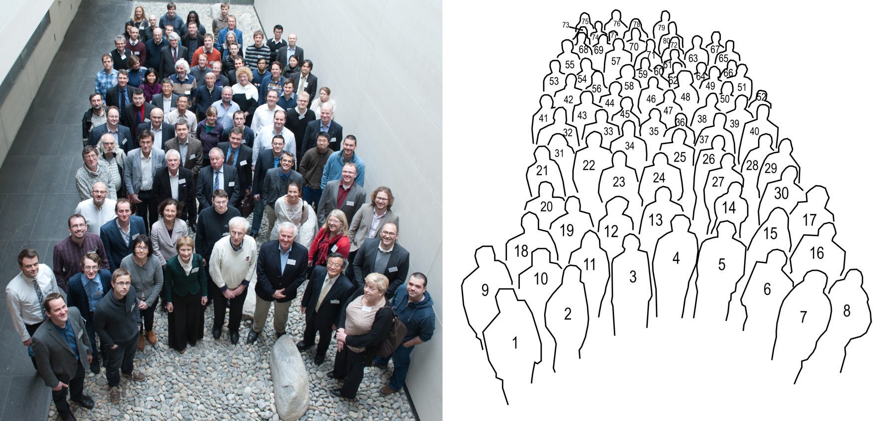
Figure 1: Group photo of the International SALVE Symposium 2015 with participants from 16 countries (to see the name of all participants click on the image).
Introduction to the SALVE symposium 2015

The introduction of the symposium was given by Ute Kaiser, who discussed the challenges of aberration-corrected transmission electron microscopy at low voltages (Fig. 2). When considering different low electron microscopic techniques, it must be taken into account that the terms "high voltage" and "low voltage" stand for different ranges. For a TEM and scanning TEM this is very low, but for a SEM this is a common voltage and for LEEM this voltage is very high. Today, atomic-resolution low-voltage AC-TEM has reached the voltage range, which is typical for SEM.
1st session, chaired by Ute Kaiser on Tuesday, February 17th

In the first talk, Peter Hartel from CEOS company, Germany highlighted the path of discoveries from the early Darmstadt project to the SALVE project. He mentioned the problems that had been solved within the Volkswagen-Foundation project, which lead to the prototype TEM hexapole corrector for Julich, and finally the obstacles which had to be overcome in the SALVE project. As the last obstacle, Hartel talked about image spread that could finally be uncovered as Johnson Nyquist noise coming from the conducting surrounding close to the image forming electrons, which is still a challenge today. View the abstract
In the second talk, David Bell from Harvard University, USA mentioned that historically higher voltage TEMs were favored since they reduce the effects of spherical and chromatic aberration; however, with the development and commercial introduction of spherical aberration correctors, electron monochromation and CC-correction have now allowed atomic resolution at much lower accelerating voltages. He outlined that low-voltage high-resolution electron microscopy has several significant advantages, including increased cross-sections for inelastic and elastic scattering, increased contrast per electron and improved spectroscopy efficiency, decreased delocalization effects and reduced radiation knock-on damage. View the abstract
In the third talk, Takanori Koshikawa from Osaka Electro-Communication University, Japan mentioned their earlier development of a novel very high brightness and high spin-polarized low energy electron microscope (SPLEEM). They have now proposed a multi-pole Wien filter which enables 3-dimensional spin operation with one device. They investigated magnetic properties of multi-layer structures with their high brightness and highly spin-polarized SPLEEM. They showed experimental and simulation results of magnetic domain images of multilayer stacks. View the abstract
2nd session, chaired by Christoph Koch on Tuesday, February 17th
In the first talk, Rafal Dunin-Borkowski from Ernst Ruska-Centre Julich, Germany mentioned the coherence of a modern field emission transmission electron microscope (TEM), which allows fascinating caustic phenomena to be observed, such as the hyperbolic umbilic catastrophe produced by a coma aberration function. He showed studies of two approximately collinear oppositely-biased metallic tips, which show rich caustic phenomena that are strongly reminiscent of the elliptic umbilic diffraction catastrophe that occurs when visible light is refracted by a water droplet with a triangular perimeter. View the abstract
In the second talk, Dirk van Dyck from University of Antwerp, Belgium, mentioned the study of beam-sensitive crystalline nanoparticles such as catalysts where there is a need for a tomographic method for fast characterization of the shape of pristine particles at atomic resolution. He described a quantitative parameterless 3D reconstruction method that uses the exit wave obtained from only one viewing direction parallel to the atomic columns. He mentioned that in this configuration the strong dynamical scattering yields a signal that is stronger than the incoherent signal in HAADF STEM. The method is based on the "channeling" theory, which is simple and provides a way to interpret the exit wave and can be visualized graphically by plotting the complex values of the pixels in complex 2D space. View the abstract
In the third talk, Ondrej Krivanek from Nion company, USA started historically with the working of aberration correctors that first appeared in the 1990's and than talked about the monochromator that was recently introduced by Nion as a part of its high energy resolution monochromated EELS-STEM (HERMES) system, with which they have successfully detected vibrational excitations (optical phonons) in a variety of materials and talked about the improvement of this new method. View the abstract
3rd session, chaired by Rafal Dunin-Borkowski on Tuesday, February 17th

In the first talk, Bohumila Lencova from Tescan company, Czech Republic, reviewed the last 20 years, since TESCAN Brno was founded, and what the company produces. She talked furthermore about the analysis of the lenses and deflectors for a correctly functioning microscope. The presentation gave an overview of approaches to charged particle optical calculations, various, displaying modes, and extended level of multi technique integration that enrich microscope functions to a new generation of imaging and analytical tool. View the abstract
In the second talk, Ai Leen Koh from Stanford University, USA highlighted a few examples in which the use of lower voltages is important when studying nanomaterials using aberration-corrected TEM, e. g. for carbon nanotubes (CNTs), which have found an increasing number of applications, most notably as field emission electron sources in X-ray tubes for medical applications. An 80 kV incident electron beam energy (which is below the threshold energy for knock-on damage in single-walled carbon nanotubes) was utilized in their study to analyze the oxidation and radiation damage processes of CNTs. View the abstract
In the third talk, Andrey Turchanin from University of Jena, Germany demonstrated how monolayers of aromatic molecules can be employed to engineer free-standing ultrathin 2D carbon materials, e.g. carbon nanomembranes (CNM). CNMs can be employed for the engineering of advanced support films for high-resolution transmission electron microscopy (HRTEM) of biological samples. Furthermore he talked about the characterization of CNMs by e.g. complementary electron spectroscopy, HRTEM and scanning tunnelling microscopy. View the abstract
4th session, chaired by Eva Olsen on Tuesday, February 17th
In the first talk, Tanja Weil from University of Ulm, Germany, referred about about biohybrid nanoparticles to achieve a nanoscale construct with exceptional macromolecular definition for nanomedicine and sensing. Through these synthetic appendages, supramolecular polypeptides and protein polymer biohybrids can be chemically programmed to possess new and improved physicochemical properties while simultaneously exhibiting unique biological behavior. They have designed multifunctional copolymers derived from proteins with stabilization of various nanoparticles such as quantum dots or nanodiamonds via multivalent interactions. A pronounced responsiveness of the emission intensity of these nanoparticles was found e.g. upon pH changes which is attractive for achieving biocompatible sensors for in vitro and in vivo applications. View the abstract
In the second talk, Elena Bichoutskaia from University of Nottingham, UK
discussed that the interpretation of HRTEM images is complicated due to continuous structure deformation caused by the imaging electron beam. A computational methodology, CompuTEM, has been implemented that takes into account the effects of the electron beam on deformation of sample structure during observation and imaging in HRTEM. The principal cause of instability of organic molecules in TEM is the low atomic weight of hydrogen and its facile atomic displacement by the e-beam. They demonstrated that the exchange of hydrogen for the heavier isotope, deuterium (doubling the atomic weight) can lead to a more than two-fold increase in stability of organic molecules in the e-beam. View the abstract
In the third talk, Tatiana Latychevskaia from University of Zurich, Switzerland reported on imaging with low-energy coherent electrons with kinetic energies in the range of 50– 250 eV that allow recording holograms and diffraction images of individual molecules. She demonstrated that individual biomolecules, such as DNA molecules, can withstand low-energy electrons radiation for hours without apparent radiation damage. The method imports the potential to distinguish between different conformations of proteins at atomic resolution. View the abstract
In the fourth talk, Andrei Khlobystov from Nottingham University, UK presented results for chemistry of individual molecules observed through a lens of
transmission electron microscope. He presented the concept of the electron beam simultaneously acting as an imaging tool and a source of energy to drive chemical transformations. In that respect, atomically thin and structurally robust carbon nanotubes serve as ultimate nanoscale test tubes, providing an imaging platform for encapsulated molecules. TEM is changing the way chemists make and study molecules. View the abstract
1st session, chaired by Dirk van Dyck on Wednesday, February 18th

In the first talk, Johannes Biskupek from Ulm University, Germany presented on the one hand side sample preparation strategies to image radiation-sensitive materials and on the other hand methods to clean graphene. To the topic radiation damage he showed two approaches: (1) sandwiching beam-sensitive objects in-between two graphene layers; and (2) isotope exchange (deuterium instead of hydrogen). Moreover he briefly showed that at low voltages imaging theories have to be newly re-thought. He moreover showed recent results on the discovery of square ice and a new phase of Au-C. View the abstract
In the second talk, Kazu Suenaga from National Institute of Advanced Industrial Science and Technology, Japan presented an experimental proof that atomic resolution can be achievable in STEM-ADF mode even at 30kV. He discussed the advantages of low voltage TEM/STEM which is the prevention of massive structural destruction. In this presentation, Suenaga summarized their recent progresses of low-voltage TEM/STEM within the scheme of the triple C project. The current status of their monochromator and aberration corrector developments were shown. The examples for atomic defect and edge analysis of low-dimensional materials was presented. View the abstract
In the third talk, Angus Kirkland from University of Oxford, UK outlined that it is essential to understand the behavior of point defects in order to deploy graphene and related materials in electronic applications. He concluded that high-resolution transmission electron microscopy is the ideal characterization tool for studying the formation and evolution of defects in graphene in real space and summarized the advances that made it possible to image defects at primary energies below those that cause significant specimen damage whilst retaining sufficient spatial resolution to resolve the local atomic configuration in the Graphene lattice around the defect site. View the abstract
In the fourth talk, Jannik Meyer from University of Vienna, Austria discussed insights to irradiation-induced modifications of graphene, which shed light onto e.g. the knock-on damage mechanism and the controlled amorphization, which provides insight to the transition from an ordered to a disordered material. He also discussed a new idea to circumvent radiation damage, based on low-dose imaging of repeatedly occuring atomic configurations. View the abstract
2nd session, chaired by Angus Kirkland on Wednesday, February 18th
In the first talk, Arkady Krasheninnikov from Aalto University, Helsinki, Finland presented the results of their first-principles theoretical studies of defects in inorganic 2D systems. He also touched upon defect production in 2D systems under impacts of energetic electrons and discussed defect and impurity-mediated engineering of the
electronic structure of 2D materials. Furthermore he addressed defects in truly one-dimensional ionic crystals, chains of CsI and also BN chains. View the abstract
In the second talk, Michael Stoeger-Pollach from Vienna University of Technology, Austria discussed that VEELS of semiconductors low beam energies have a unique advantage over high beam energies, namely the Cerenkov effect can be avoided. In their study they demonstrate bandgap measurements of various materials using 20 keV electron beam acceleration voltage. With this new set-up they improve the spatial resolution of the STEM probe. On the example of BN, they varied the beam energy in the range from 200 keV to 20 keV and compared the results with simulations. View the abstract
In the third talk, Andreas Kastenmueller from Gatan company, Germany referred about the adoption of digital cameras for TEM imaging as a replacement for film in the last 25 years. The development by Gatan has now passed an inflection point in resolving the core issues that have limited performance of TEM digital imaging systems on a cost/performance basis. He summarized that the gains have been integrated into the architecture of next-generation TEM cameras and that microscopists can now leverage these core technologies to drive TEM imaging performance which increases resolution, frame rate, and "video" outputs for in-situ reactions. View the abstract
3rd session, chaired by Harald Rose on Wednesday, February 18th
In the first talk, Annick Loiseau from Laboratoire d'etude des microstructures, France discussed that until recently, properties of h-BN materials were poorly known due to both the scarcity of crystals and suitable investigation tools. However, this situation has changed: (1) the development of dedicated photoluminescence and cathodoluminescence experiments has been adapted to the detection in the far UV range, and (2) high quality single crystals are available. Thanks to these facts, she concluded, the optical properties of h-BN could be analyzed. In the talk, Loiseau presented excitonic luminescence as a qualification parameter of the defect densities present in the layers. Furthermore she showed that EELS provides an alternative approach to the nature of electronic excitations by inspecting the low losses. View the abstract
In the second talk, Ing-Shouh Hwang from Academia Sinica Nankang, Taiwan discussed low-energy electron diffractive imaging based on a single-atom electron source. He proposed several transmission-type schemes, both for lens-less and with-lens designs. However, several schemes can only study samples with thickness less than 1 nm due to the electron energy between 20-500 eV. He concluded that it is thus desirable to increase the electron energies to 1-10 keV. View the abstract
In the third talk, Weishi Wan from Lawrence Berkeley National Laboratory, USA discussed the design for an aberration-corrected, ultrafast spin-polarized LEEM with multiple electron sources. He described a high-resolution aberration-corrected LEEM/PEEM combined with a high temperature Scanning Tunnelling Microscopy (HT-STM) platform. He presented results with the cold FE source, which show spatial resolution below 2 nm,
while also achieving atomic resolution with the HT-STM running concurrently with the LEEM
instrument. View the abstract
In the fourth talk, Eva Olsson from Chalmers University, Sweden reported on electron beam enhanced thermal stability of polymer photovoltaic blends. Her talk addressed studies of the effect of thermal annealing of microstructures and the use of the electron beam in a transmission electron microscope (TEM) to enhance the thermal stability. Furthermore she presented the effect of the electron beam exposure and the influences of acceleration voltage on the microstructural evolution. View the abstract
The symposium was finished with a round table discussion directed by Ute Kaiser about the different needs of industrial and academic research and the possible future trends that should be addressed by the electron microscopy manufactures. The discussion was introduced by BASF (Philipp Muller), JEOL (Philipp Wachsmuth and Manuel Reinhard) and by FEI (Stefan Kujawa). The general tenor was that we need specialized microscopes nowadays and SALVE will be one of the big challenges for future. At the end we are aiming to an automated tunable fully corrected low-medium voltage microscope. However we know: There is plenty of work to be done and "science never solves a problem without creating ten more." (George Bernard Shaw).
Overall both, birthday celebration and symposium were a great successes. A subsequent SALVE symposium is planned for early 2017. The organizers are extremely grateful to the donations and sponsorships of CEOS, DGE, FEI, Gatan, Hitachi, Jeol, Nion, Tescan, Technical University of Darmstadt and ZEISS.