Utrasharp 1D p–n Junction Electronic Devices from One-Pot Chemical Vapor Deposition Synthesis
May 04, 2021 - Lateral heterostructures of dissimilar monolayer transition metal dichalcogenides provide great opportunities to build 1D in-plane p–n junctions for sub-nanometer thin low-power electronic, optoelectronic, optical, and sensing devices. A team of scientists from the Universities of Jena and Ulm, the IPHT and the Abbe Center of Photonics in Germany, as well as the University of Cambridge in the UK, has fabricated these lateral heterostructures using an easily applicable high quality chemical vapor deposition (CVD) approach and demonstrated their applicability in new devices.
For realizing sub-nanometer atomically thin devices such as diodes,[1, 2] photodetectors,[1, 3] photovoltaic devices,[4] as well as electroluminescent,[1, 4] and quantum devices[1] transition metal dichalcogenides (TMD) architectures have been proposed. 1D lateral heterostructures can also be used to study physical phenomena under extreme confinement, which are not observable otherwise and may lead to new device applications.
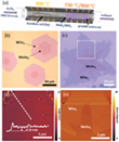
Typically, a one-step[5, 6] or a two-step[7] growth procedure either by physical vapor deposition (PVD)[5] or by chemical vapor deposition (CVD) is employed for growing TMD lateral heterostructures by lateral edge epitaxy.[6] A two-step growth procedure in which regions of different TMDs are grown one after another in subsequent growth experiments is the most common approach for obtaining TMD lateral heterostructures.[7] However, this method is difficult to scale up and the TMD layer grown initially has to be exposed to ambient conditions for the preparation of the second growth, which may have detrimental effects to the interface. The team now used a one-step CVD approach to fabricate the 1d p-n junctions. The 1D p-n junctions were formed employing a Knudsen type effusion cell to deliver the chalcogen precursors for the growth of the lateral heterostructures.[8] This technique has been shown to produce high-quality transition metal disulfide monolayers.[9] A scheme of the CVD setup is presented in Figure 1a.
A detailed characterization of a one-pot CVD-grown large area MoSe2-WSe2 lateral heterostructure by low-voltage aberration-corrected high-resolution transmission electron microscopy (HRTEM), high-angle annular dark-field scanning transmission electron microscopy (HAADF- STEM) as well as energy-dispersive X-ray spectroscopy (EDX) electron microscopy (LV-AC-HRTEM) has given scientists rare insight into the formation of the interface between the two different transition metal dichalcogenide materials. Optical microscopy (OM), Raman spectroscopy, atomic force microscopy (AFM), and photoluminescence (PL) spectroscopy were applied in addition for probing their morphological, structural, and optical properties. The authors then realized atomically thin electronic and optoelectronic p–n junction devices showing their potential new applicability.
Characterization by STEM-EDX and HRTEM
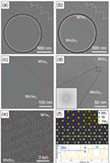
HAADF-STEM with EDX as well as chromatic (Cc) and spherical (Cs) aberration-corrected HRTEM was used to characterize the lateral MoSe2-WSe2 heterostructure interface, see Figure 2. The interface images unambiguously confirmed the formation of a monolayer heterostructure, see Figure 3, whereas the formation of large-sized MoSe2 and WSe2 areas, as well as a very straight boundary could also be clearly revealed. The contrast analysis in Figure 2a and the respective EDX maps in Figure 2b,c indicate that Se is homogeneously distributed on the whole heterostructure area, whereas Mo and W are present in the inner and outer regions, respectively, as expected.
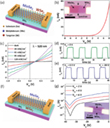
Monolayer lateral heterostructures of n-type MoSe2 and p-type WSe2 enable the realization of atomically thin electronic and optoelectronic p–n junction devices in two different configurations as shown schematically in Figure 4a,f. In the first type of device, the p-type WSe2 and n- type MoSe2 areas are connected in series, a current–voltage (I–V) characteristic of such a p–n junction diode device is shown in Figure 4b (Inset of 4b shows OM image). The rectification behavior of the diode can be observed from the I–V characteristics (i.e., the diode allowed electrical conduction only when it is operated in forward bias). In Figure 4c, the I–V characteristics of a p–n junction device under dark and under illumination with varying intensities of the laser are shown. The device exhibits a dark current of 135 pA at a source-drain bias (Vds) of 1 V. When irradiating the device, a clear photovoltaic effect can be observed. For instance, when irradiating with an intensity of 61 ± 5 mW cm−2 the device shows an open-circuit voltage (VOC) of 0.24 V and a short-circuit current (ISC) of 354 pA. The power conversion efficiency (PCE), is calculated as 0.12%, which is similar to the reported values on similar TMD-based junctions.[11] The onset of the photocurrent was found at a photon energy of 2.35 eV, just below the 520 nm of the laser light applied experimentally. However, the calculations also show that the photocurrent is sensitive to the doping level of the devices and to the defect concentration. For a doped junction, the onset of the photocurrent was found at a lower photon energy of 2.15 eV and the photocurrent is larger compared to the undoped junction. Hence, this result can be considered as a qualitative proof of the applicability of the heterostructures devices in a photovoltaic cell. The figures of merit of the heterostructure photodetector are comparable to previously reported photodetectors fabricated using TMD-based materials and junctions.[12] When operating at the photovoltaic mode, the photodetector shows a high on/off ratio in the order of 104, which is higher than most of the previously reported TMD-based photodetectors.
Another type of devices was also fabricated so that the MoSe2 and WSe2 areas were connected in parallel to the source-drain electrodes as shown schematically in Figure 3f. The junction between the p and n region is in the middle perpendicular to the electrodes. Such devices with parallel p-type (WSe2) and n-type (MoSe2) channels are expected to function as ambipolar field-effect transistors.[13] The ambipolar transistors are promising building blocks for applications including lighting, display, memory, logic, and neuromorphic computing devices.[ An OM image of an ambipolar transistor is shown in the inset of Figure 4g. We performed field-effect transport measurements on such devices and transfer characteristics, that is, the enhancement of drain current with applied Vg at different applied Vds, are shown in Figure 4g. The transfer characteristics demonstrate ambipolar transport as expected. In such a device configuration, the p-channel (WSe2) becomes conductive towards negative Vg and the MoSe2 n-channel becomes conductive towards more positive Vg. It can be seen that the minimum conductivity points of the transfer curves shifted towards the negative gate voltages possibly due to substantial n-doping induced by the SiO2 substrate as well as the transfer process.[14]
The 1D p–n junctions can be used as rectifiers, solar cells, self-powered photodetectors, and light-emitting diodes. “Using TEM, we have confirmed the high quality of 1D boundary between the MoSe2 and WSe2 in their lateral heterostructure,” Ute Kaiser said. The authors demonstrated the possibility of ambipolar field-effect transistors using laterally connected parallel MoSe2-WSe2 channels. We expect that many new discoveries will also come from the further study the impact of the dimensionality on the dynamics of excitations in the 1D solid- state boundaries, where many possible new applications in sub-nanometer, non-silicon electronic, optoelectronic, and photovoltaic devices are to be expected to come in the future.
Resource: Najafidehaghani, E., Gan, Z., George, A., Lehnert, T., Ngo, G. Q., Neumann, C., Bucher, T., Staude, I., Kaiser, D., Vogl, T., Hübner, U., Kaiser, U., Eilenberger, F. & Turchanin, A. (2021). 1D p–n Junction Electronic and Optoelectronic Devices from Transition Metal Dichalcogenide Lateral Heterostructures Grown by One‐Pot Chemical Vapor Deposition Synthesis. Advanced Functional Materials, 2101086. https://doi.org/10.1002/adfm.202101086
-
R. Frisenda, A. J. Molina-Mendoza, T. Mueller, A. Castellanos-Gomez, H. S. J. van der Zant, Atomically thin p-n junctions based on two-dimensional materials. Chem. Soc. Rev. 2018, 47, 3339.
-
L. Liu, N. Xu, Y. Zhang, P. Zhao, H. Chen, S. Deng, Van der Waals Bipolar Junction Transistor Using Vertically Stacked Two- Dimensional Atomic Crystals. Adv. Funct. Mater. 2019, 29, 1807893;
-
W. Wu, Q. Zhang, X. Zhou, L. Li, J. Su, F. Wang, T. Zhai, Self-powered photovoltaic photodetector established on lateral monolayer MoS2-WS2 heterostructures. Nano Energy 2018, 51, 45.
-
A. Pospischil, M. M. Furchi, T. Mueller, Photovoltaic effect in an electrically tunable van der Waals heterojunction. Nat. Nanotechnol. 2014, 9, 257.
-
C. Huang, S. Wu, A. M. Sanchez, J. J. P. Peters, R. Beanland, J. S. Ross, P. Rivera, W. Yao, D. H. Cobden, X. Xu, Lateral heterojunctions within monolayer MoSe2-WSe2 semiconductors. Nat. Mater. 2014, 13, 1096.
-
F. Ullah, Y. Sim, C. T. Le, M.-J. Seong, J. I. Jang, S. H. Rhim, B. C. Tran Khac, K.-H. Chung, K. Park, Y. Lee, K. Kim, H. Y. Jeong, Y. S. Kim, Growth and simultaneous valleys manipulation of two-dimensional MoSe2-WSe2 lateral heterostructure. ACS Nano 2017, 11, 8822.
-
K. Chen, X. Wan, J. Wen, W. Xie, Z. Kang, X. Zeng, H. Chen, J.-B. Xu, Electronic properties of MoS2-WS2 heterostructures synthesized with two-step lateral epitaxial strategy. ACS Nano 2015, 9, 9868.
-
A. George, C. Neumann, D. Kaiser, R. Mupparapu, T. Lehnert, U. Hübner, Z. Tang, A. Winter, U. Kaiser, I. Staude, A. Turchanin, Controlled growth of transition metal dichalcogenide monolayers using Knudsen-type effusion cells for the precursors. J. Phys.: Mater. 2019, 2, 016001.
-
S. Shree, A. George, T. Lehnert, C. Neumann, M. Benelajla, C. Robert, X. Marie, K. Watanabe, T. Taniguchi, U. Kaiser, B. Urbaszek, A. Turchanin, High optical quality of MoS2 monolayers grown by chemical vapor deposition. 2D Mater. 2019, 7, 015011.
-
X. Wang, Y. Gong, G. Shi, W. L. Chow, K. Keyshar, G. Ye, R. Vajtai, J. Lou, Z. Liu, E. Ringe, B. K. Tay, P. M. Ajayan, Chemical vapor deposition growth of crystalline mono layer MoSe2. ACS Nano 2014, 8, 5125.
-
S. Jia, Z. Jin, J. Zhang, J. Yuan, W. Chen, W. Feng, P. Hu, P. M. Ajayan, J. Lou, Lateral Monolayer MoSe2–WSe2 p–n Heterojunctions with Giant Built-In Potentials. Small 2020, 16, 2002263;
-
M. Long, P. Wang, H. Fang, W. Hu, Progress, Challenges, and Opportunities for 2D Material Based Photodetectors. Adv. Funct. Mater. 2019, 29, 1803807.
-
Y. Ren, X. Yang, L. Zhou, J.-Y. Mao, S.-T. Han, Y. Zhou, Recent Advances in Ambipolar Transistors for Functional Applications. Adv. Funct. Mater. 2019, 29, 1902105.
-
M. Amani, M. L. Chin, A. L. Mazzoni, R. A. Burke, S. Najmaei, P. M. Ajayan, J. Lou, M. Dubey, Growth-substrate induced performance degradation in chemically synthesized monolayer MoS2 field effect transistors. Appl. Phys. Lett. 2014, 104, 203506.


